
Introduction
The modern form of the Solar cell was invented in 1954 at Bell Telephone Laboratories. Today there are wide range of PV cell technologies in the market which are classified into three generations, depending on the basic material (photo sensitive material) used and the level of commercial maturity.
First-generation PV systems use the wafer-based crystalline silicon (c-Si) technology. This type of PV cell is also called the bulk material cell. This type of cell is mostly used for terrestrial application.
Second-generation PV systems are based on thin-film PV technologies. These are also called the thin film cells. These include 1) amorphous (a-Si) and micromorph silicon (a-Si/µc-Si); 2) Cadmium Telluride (CdTe); and 3) Copper-Indium-Selenide (CIS) and Copper-Indium-Gallium-DiSelenide (CIGS). Thin film PV cells are under early market deployment.
Third-generation PV systems include technologies such as Concentrating Photovoltaic (CPV) and Organic PV cells that are still under demonstration or have not yet been widely commercialised.
Current market share of wafer-based crystalline silicon(c-Si) is 85%-90% of global PV module sale whereas the market share of PV modules based on Thin film technologies is 10%-15%.
Global Thin film module production capacity has increased significantly since 2007 although the price of wafer-based crystalline silicon(c-Si) has sharply decreased. There has been discussion around the relative merits of both.
The objective of this paper is to compare the manufacturing processes involved in the manufacturing of Thin film Solar cells vis-a-vis Bulk film solar cells.
Crystalline Silicon PV Technologies (c-Si)
Crystalline silicon PV cells are the most common solar cells used in commercially available solar panels, representing more than 85% of world PV cell market sales in Crystalline silicon PV cells have laboratory energy conversion efficiencies over 25% for single-crystal cells and over 20% for multicrystalline cells. However, industrially produced solar modules currently achieve efficiencies ranging from 18%–22% under standard test conditions. Manufacturing process for crystalline Silicon Solar cell is as per the flow chart given in Fig. 1.
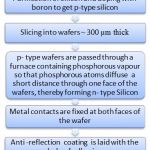 |
Figure 1: Process flow chart for manufacturing of crystalline PV Solar cell |
Thin Film PV Technologies
Thin film deposition is a process in which the physical characteristics of a surface are modified by applying a very thin coating often just a few millionth of a millimetre thick. The surface is known as the substrate.
The films can be used to modify the optical characteristics of a surface, its electrical conductivity, hardness, lubricating property, to provide corrosion resistance or chemical inertness, or simply decoration.
A thin-film Solar cell (TFSC), also called thin film photovoltaic cell (TFPV) is a Solar cell that is made by depositing one or more thin layers (Thin Film ) material on a substrate.
Many different photovoltaic materials are deposited with various deposition methods on a variety of substrate.
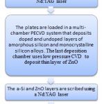
Manufacturing process for a-silicon Thin film Solar cell used by BP Solar is as per the flow chart given in Fig. 2.
 |
Comparison between Thin Film PV and Wafer based PV manufacturing technologies
The main advantages of manufacturing process for a-silicon Thin film solar cell are the following.
- The technique is suitable for high automation
- Large size cells can be fabricated
- Potential of reducing manufacturing costs is high
- Low capital investment
- Faster deploymen
Conclusion
Most of the effort is now centred on thin film deposition rather than wafer based modules, although there is still discussion around the relative merits of both. The main arguments in favour of thin film are that it uses less photovoltaic material is much faster and simpler to produce than the complex and delicate process of producing wafer based bulk material cell.
References
- Sukhatme S P ”Solar Energy- Principles of Thermal Collection and Storage”, Tata McGraw-Hill Publishing Company Limited, New Delhi
- Khan B H, “Non-Conventional Energy Resources”, Tata McGraw-Hill Publishing Company Limited, New Delhi
- “Renewable Energy Technologies : Cost Analysis Series”, IRENA Working Paper, Volume 1: Power Sector Issue 4/5, Solar Photovoltaics, International Renewable Energy Agency
- Carlson David E., Wronski Christopher R., “Amorphous Silicon Solar Cells”, Solar Cells Materials, Manufacture and Operation, Elsevier
- Osterwald Carl R., “Standards Calibration and Testing of PV Modules and Solar Cells”, Solar Cells Materials, Manufacture and Operation, Elsevier